

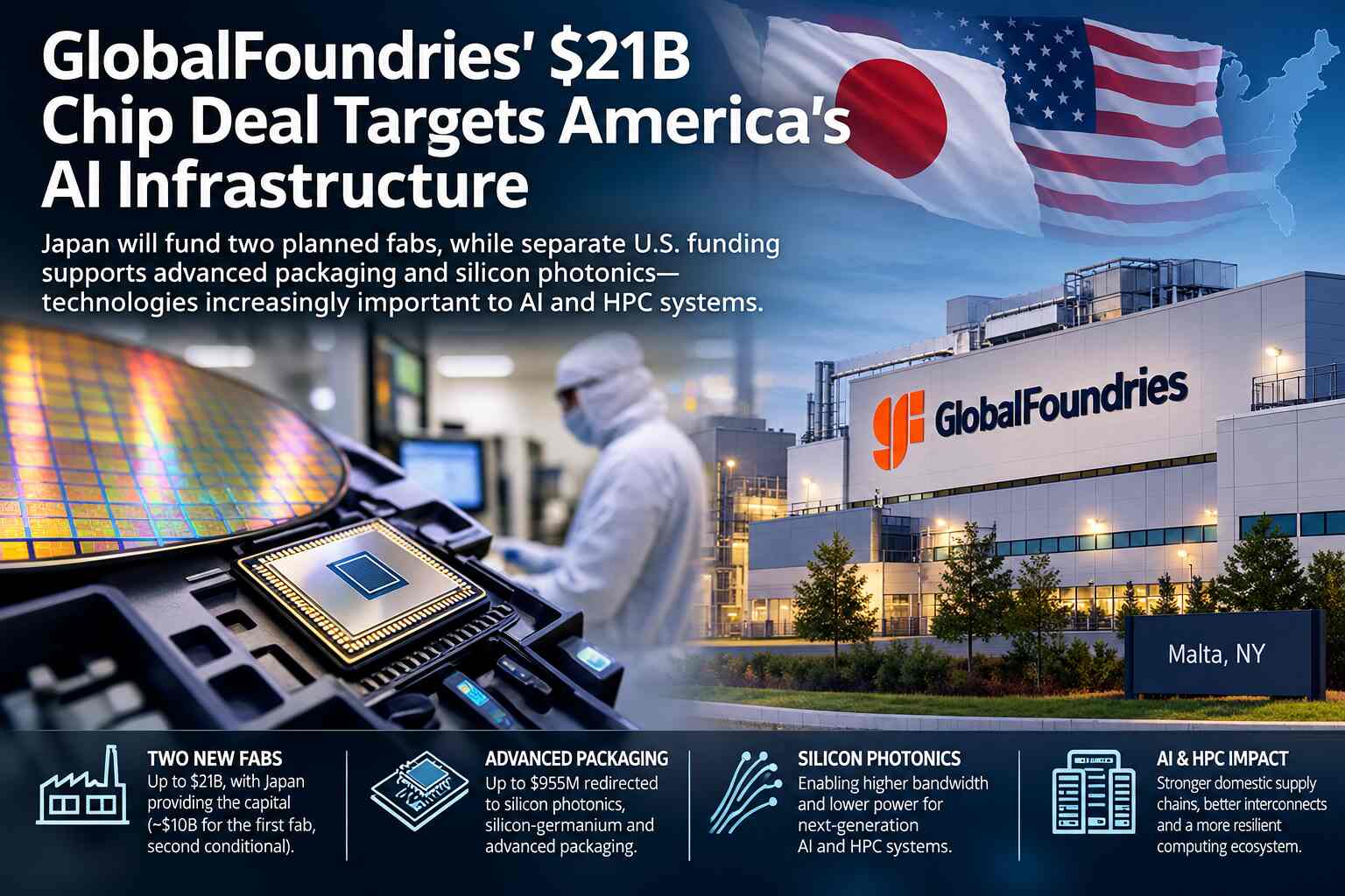
Japan will fund two planned fabs, while separate U.S. funding supports advanced packaging and silicon photonics, technologies increasingly important to AI and HPC systems.
Under a U.S.-Japan initiative valued at up to $21 billion, GlobalFoundries is slated to operate two semiconductor fabrication facilities in Malta, New York. While Japan provides the necessary capital, the construction of the second facility remains contingent upon future market demand. Concurrently, a separate, perhaps more immediate strategic development for the AI and high-performance computing (HPC) sectors involves the reallocation of up to $955 million in existing CHIPS Act funding. These funds will be directed toward advancing packaging, silicon photonics, and silicon-germanium technologies.
It is critical to distinguish between these two initiatives: the new fabs are designed for foundational semiconductor production rather than leading-edge AI processors, whereas the packaging investment addresses the increasingly vital challenge of data movement and chip connectivity as AI systems scale.
Collectively, these agreements reflect a strategic effort to enhance U.S. semiconductor capacity; however, the extent to which they alleviate supply-chain constraints will depend on production timelines, customer commitments, and actualized capacity. The headline figure of $21 billion warrants closer scrutiny, as the initial investment is approximately $10 billion, with the second phase tied to market conditions. Furthermore, GlobalFoundries will operate the facilities as a technology provider rather than as the owner.
Simultaneously, the reallocation of $955 million to GlobalFoundries’ existing facilities in Malta and Burlington, Vermont, carries significant implications for the supercomputing industry. As AI systems scale, performance is increasingly dictated by the technologies that manage data transmission between processors, memory, and networking systems. Consequently, these announcements represent two distinct but complementary investments: one focused on expanding foundational manufacturing, and the other on strengthening the bandwidth and connectivity infrastructure essential for future AI and HPC systems.
The supercomputer is more than its processors
The semiconductor industry has spent years concentrating on accelerator performance, transistor density, and the race to develop increasingly powerful AI processors. Yet the largest computing systems face a broader engineering challenge.
An accelerator can perform enormous numbers of calculations, but its practical contribution to a distributed workload depends on how quickly data reaches it, how efficiently results move between devices, and how effectively the surrounding system manages power and heat.
Advanced packaging has become central to this problem. Modern high-performance processors can combine multiple compute and memory components within tightly integrated packages. Silicon interposers provide dense connections between dies, enabling the high-bandwidth interfaces required by complex multi-die designs.
These components do not independently make a processor faster. Their value comes from enabling the integration and data movement that a high-performance architecture requires.
GlobalFoundries' separate agreement with Taiwan Semiconductor Manufacturing Co. (TSMC), announced October 8, illustrates the point. The companies announced a multiyear agreement valued at $2 billion under which GlobalFoundries will manufacture silicon interposers for TSMC's Chip-on-Wafer-on-Substrate (CoWoS) advanced-packaging ecosystem. GlobalFoundries expects production to ramp in the first half of 2028.
The arrangement establishes a planned U.S.-based manufacturing source for an important component of advanced AI packaging. It does not, however, mean that GlobalFoundries will manufacture TSMC's leading-edge AI processors or perform every stage of final assembly and packaging.
That distinction matters. A domestic source of interposers can strengthen one part of the supply chain without eliminating dependence on other manufacturers, packaging operations or specialized equipment.
For HPC system designers, the practical question is whether the additional capacity will deliver the components, yields, manufacturing consistency and production volumes needed to support increasingly complex accelerator systems.
The announcement establishes an industrial objective. It does not yet provide enough public information to quantify the resulting improvement in AI-system performance or supply availability.
Silicon photonics and the interconnect challenge
The $955 million federal award reallocation targets another increasingly important part of the computing stack: moving data efficiently between devices.
Silicon photonics uses optical technology to transmit information, while silicon-germanium technologies support specialized semiconductor applications, including high-frequency electronics. Both are relevant to communications infrastructure and data-center systems.
As accelerator clusters grow, communication networks must move increasing quantities of data between compute nodes and across the broader facility. Electrical interconnects remain essential, but their power consumption, reach, and bandwidth constraints create pressure to develop more efficient optical technologies.
Near-packaged optics and co-packaged optics are among the approaches being developed to bring optical connectivity closer to switching or computing silicon. Their potential benefits include improved bandwidth density and reduced energy consumed by portions of the data-movement infrastructure.
Those benefits are not automatic. They depend on the implementation, optical components, packaging approach, thermal characteristics, manufacturing yield, and system-level design.
GlobalFoundries has already described its silicon-photonics work as part of a broader effort to support next-generation AI and HPC connectivity. Its existing capabilities in Malta and Burlington will receive investment under the amended federal award.
The critical point is that the $955 million is not a new federal award added on top of the existing CHIPS funding. The Commerce Department is reallocating up to that amount from GlobalFoundries' existing $1.5 billion award. GlobalFoundries has agreed to increase its own capital investment in the facilities covered by the amendment to $5 billion.
Commerce says the revised allocation will support technologies increasingly important to data centers and communications infrastructure.
What remains unclear is how quickly the investments will translate into high-volume production, which specific technologies will reach commercial maturity first, and how much capacity will be available to customers building large AI systems.
The $21 billion headline needs qualification
The proposed fabs represent a substantial manufacturing expansion, but the financial structure deserves more careful examination than a headline announcing a $21 billion investment might suggest.
Japan will provide the capital for the two facilities. The initial project involves approximately $10 billion and is expected to begin operations in 2029. The additional approximately $10 billion associated with the second facility depends on a decision expected before the end of 2028, tied to market demand.
The combined target is approximately 900,000 300-millimeter wafers of annual capacity per fab when fully operational. If both facilities proceed and reach their stated capacity, the initiative could add approximately 1.8 million wafers of annual capacity.
Those figures are targets, not current production. Nor do they establish how much usable semiconductor output will result, which products will be manufactured at particular process nodes, or how much capacity individual customers will secure.
GlobalFoundries describes the new facilities as foundational semiconductor production intended to support automotive, industrial and connected-infrastructure markets. The company has not disclosed the specific process nodes for the two fabs.
They should therefore not be presented as new leading-edge AI-processor factories.
The business model also differs from a conventional expansion financed and owned by the manufacturer. GlobalFoundries will act as technology provider and operator, earning construction-management fees, ongoing operating fees and technology-licensing revenue.
The company expects approximately $50 million in construction-management revenue in 2027. It has also indicated that its fee-generating relationship with the facilities is intended to extend for at least 20 years.
That arrangement could give GlobalFoundries a long-term revenue stream without requiring it to own the facilities. But the available disclosures do not quantify the full expected operating and licensing economics, the ultimate profitability of the projects, or the risks associated with executing the manufacturing ramp.
The financial distinction is important: The total project funding is not equivalent to revenue for GlobalFoundries, and neither figure should be confused with profit.
Washington becomes a shareholder
The Japan-funded fab initiative also arrives alongside a separate change in the U.S. government's relationship with GlobalFoundries.
Under another agreement, the Commerce Department will receive an equity stake of approximately 4% in the company. GlobalFoundries CEO Tim Breen has separately described total U.S. government ownership as approximately 7%.
The precise terms of the new equity arrangement, including the purchase price, voting rights, board representation and exit provisions, have not been fully disclosed in the materials available for this report. The reported total ownership figure also requires reconciliation against the previously disclosed government equity positions.
These questions matter because government equity creates a different relationship from a conventional grant. Taxpayers may participate in the company's financial upside, but the public also needs clarity about the terms, governance, and objectives of that participation.
The fab arrangement introduces another layer. Japan supplies the capital for facilities that GlobalFoundries operates, while the U.S. and Japanese sides participate in the investment's ownership and financial returns.
Under the reported structure, available free cash flow is divided equally between the U.S. and Japan until a specified allocation threshold is reached, after which 90% goes to the U.S. Japan is expected to recover its principal and interest first.
The full terms, including the threshold and the precise governance arrangements, remain important unanswered questions.
The structure reflects a wider policy experiment: using international capital and public-sector participation to expand domestic industrial capacity while seeking financial returns for the participating governments.
Whether that model becomes a durable template for semiconductor infrastructure will depend on its execution, its economics and the extent to which the resulting facilities deliver the strategic capabilities promised.
The demand question cannot be ignored
GlobalFoundries expects the initiative to support demand across automotive, industrial and connected-infrastructure markets. The company's announcement also identifies Renesas Electronics and Apple as initial customers or customer interests, but public disclosures do not establish firm production volumes or detailed offtake terms.
Those distinctions matter when evaluating a manufacturing expansion of this scale.
Semiconductor factories are long-lived assets that require substantial investment, specialized equipment, skilled workers, and sustained utilization. Building capacity ahead of demand can provide supply-chain resilience, but it can also create financial pressure if customer requirements do not develop as anticipated.
The second fab's conditional status acknowledges that risk. GlobalFoundries' leadership has indicated that the company will not proceed if the market is insufficient.
For policymakers, that raises a central question: how should strategic capacity be valued when its benefits include supply-chain resilience and national security, but its commercial returns depend on future demand?
For HPC operators, the question is more immediate. Will the new facilities and the separate advanced-packaging investments deliver components that are difficult to obtain today, or will they primarily expand capacity in semiconductor categories that do not directly address the most acute constraints in AI infrastructure?
The answer will depend on the products, customers, and production schedules that emerge from the projects.
Three timelines, not one
The announcements also involve distinct schedules that should not be conflated.
The GlobalFoundries-TSMC silicon-interposer agreement targets a production ramp in the first half of 2028. The first Japan-funded fab is expected to begin operating in 2029. The separate photonics, SiGe, and advanced-packaging expansion under the amended CHIPS award does not have a single publicly specified completion date in the announcement.
The interposer manufacturing expansion is associated with GlobalFoundries' existing Malta campus, not simply with the two proposed Japan-funded fabs. Nor does the 2029 timeline for the new facilities establish that they will manufacture the components covered by the TSMC agreement.
This is more than a scheduling detail. Semiconductor supply chains depend on coordination between wafer production, packaging, testing, component qualification, and final system integration. A facility coming online does not mean every part of the surrounding supply chain will be ready at the same time.
The industry will need evidence of completed equipment installation, qualified processes, customer acceptance and reliable production before projected capacity can be treated as operational supply.
What the deal must prove
The expansion led by GlobalFoundries represents a significant development in the broader effort to fortify U.S. semiconductor manufacturing. The integration of Japanese capital, established manufacturing expertise, and targeted public investment has the potential to enhance critical capabilities for future computing and communications systems.
The long-term impact of these initiatives hinges on meeting development timelines, aligning capacity with market demand, and achieving cost-effective, high-yield production in advanced packaging and silicon photonics.
Furthermore, the company and relevant government agencies must provide greater transparency regarding process technologies, customer commitments, equity terms, and the structural relationship between public funding and private commercial agreements. Descriptions of the planned interposer capacity as the inaugural U.S.-based source for advanced packaging should be viewed with precise qualification; official government endorsements do not serve as independent technical verification of competitive market capabilities.
For the supercomputing trade, the broader implication is that the AI infrastructure race cannot be evaluated solely through announced investments or production volumes. Success must be measured by the operational capacity to manufacture, interconnect, and deploy the essential components required for large-scale computing systems.
The $21 billion initiative is a substantial strategic bet on semiconductor capacity. Its actual significance for AI and high-performance computing will depend on whether this output, bolstered by investments in photonics and advanced packaging, effectively alleviates existing constraints within the computing supply chain. Until production timelines, customer commitments, and financial terms are further clarified, this agreement should be viewed as a major industrial commitment whose technical and economic efficacy remains to be proven.