Researchers at The City College of New York have discovered a novel way to manipulate defects in semiconductors. The study holds promising opportunities for novel forms of precision sensing, or the transfer of quantum information between physically separate qubits, as well as for improving the fundamental understanding of charge transport in semiconductors. 
{module title="INSIDE STORY"}
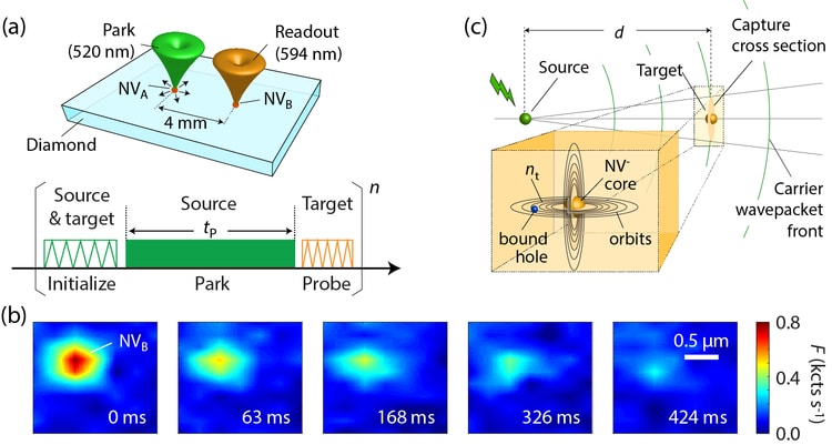
Using laser optics and confocal microscopy, the researchers demonstrated that they could make one defect eject charges – holes – under laser illumination allowing the other defect several micrometers away to catch them. The charge state of the latter defect is then altered from a negative into a neutral one via a charge capture.
The study utilized a special type of point defect—nitrogen-vacancy center in diamond. These color centers possess spin—an inherent form of angular momentum carried by elementary particles—making them attractive for quantum sensing and quantum information processing. The researchers used a specific protocol to filter out the charges originating solely from the nitrogen-vacancy based on its spin projection.
“The key was isolating the source defect, with only the nitrogen-vacancy being present, which we achieved by making charge ejection conditional on the defect’s spin state,” said Artur Lozovoi, physics postdoctoral researcher in CCNY’s Division of Science and the paper’s lead author. “Another crucial aspect was having a “clean” diamond with as few defects as possible. Then, the long-range attractive Coulombic interaction between a defect and a hole substantially increases the probability of the charge going towards the target, which ultimately made our observations possible.”
The present study uncovered that in the clean material the charge transport efficiency is a thousand times higher than observed in previous experiments, a phenomenon characterized by the researchers as a “giant capture cross-section”. This discovery could pave the way towards establishing a quantum information bus between color center qubits in semiconductors.
“This process of a charge capture by an individual defect has only been described theoretically before,” added Lozovoi. “There is now an experimental platform that enables us to look into how these defects interact with free charges in crystals and how we can use it for quantum information processing.”


 How to resolve AdBlock issue?