Snowflake's $6 Billion AWS bet signals the next phase of enterprise AI infrastructure

Enterprise artificial intelligence is rapidly evolving from experimentation into full-scale operational deployment, and Snowflake is making one of the industry’s largest infrastructure commitments to accelerate that transition.
 
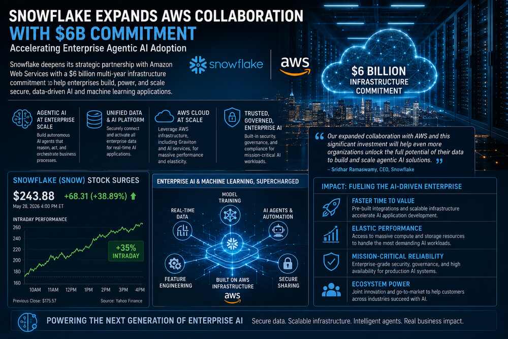
This week, the AI data cloud company announced an expanded strategic collaboration with Amazon Web Services, including a massive $6 billion multi-year infrastructure commitment to accelerate enterprise adoption of generative and agentic AI technologies.
 
The announcement immediately electrified investors. Snowflake’s stock surged more than 39% today following stronger-than-expected earnings and the AWS partnership expansion, marking one of the company’s strongest single-day market performances since its IPO.
 
For the supercomputing and enterprise HPC markets, the agreement represents something larger than a cloud partnership. It signals the emergence of AI-native enterprise infrastructure, in which massive-scale data platforms, hyperscale compute, and autonomous AI agents increasingly operate as a unified system.

From data warehousing to AI operating platform

Snowflake originally built its reputation as a cloud-native data warehousing company. But the modern AI race is forcing enterprise platforms to evolve far beyond analytics.
 
The new AWS agreement reflects that shift.
 
According to the announcement, the partnership focuses heavily on deploying “agentic AI” systems directly against enterprise data repositories, allowing organizations to build AI-driven applications that can reason over governed corporate datasets, automate workflows, and execute business processes securely at scale.
 
That distinction does matter.
 
Traditional enterprise AI systems primarily generated predictions or summaries. Agentic AI systems instead perform actions autonomously, orchestrating tasks, interacting with software systems, managing workflows, and continuously adapting using real-time enterprise data.
 
This dramatically increases infrastructure demands.
 
Unlike consumer chatbots, enterprise agentic AI workloads require:
  • Persistent access to structured and unstructured corporate data
  • High-throughput cloud storage systems
  • Distributed GPU and AI accelerator resources
  • Low-latency inference pipelines
  • Fine-grained governance and security controls
  • Continuous orchestration across thousands of simultaneous tasks
These are effectively supercomputing-scale operational problems being pushed into mainstream enterprise IT.

Why AWS matters

Snowflake’s decision to commit $6 billion to AWS infrastructure is not merely a purchasing agreement, it is a strategic acknowledgment that enterprise AI adoption will require hyperscale compute capacity on a sustained basis.
 
The company specifically highlighted growing enterprise demand for AI and data workloads running on AWS, including Graviton compute infrastructure and AI processing services.
 
This reflects a broader trend across the AI industry: compute-intensive machine learning is increasingly consuming cloud infrastructure at a scale once associated primarily with scientific supercomputing centers.
 
Enterprise AI deployment now depends on many of the same architectural principles that drive modern HPC systems:
  • Massive parallel processing
  • Distributed memory management
  • High-bandwidth data pipelines
  • Accelerator-rich architectures
  • Scalable orchestration frameworks
  • Optimized interconnect performance
The boundary between enterprise cloud computing and supercomputing is steadily dissolving.

Enterprise AI is entering its production phase

The market reaction suggests investors increasingly believe enterprise AI spending is shifting from pilot projects to production-scale deployment.
 
Snowflake reported strong fiscal Q1 2027 results alongside the AWS announcement, helping trigger the stock rally. Analysts cited accelerating AI demand, rising customer adoption, and expanding enterprise workloads as key growth drivers.
 
As of today, Snowflake shares traded near $244, up dramatically from the prior close of around $175.
 
The rally is particularly notable because Snowflake spent much of the past year under pressure amid concerns about slowing cloud optimization spending and intensifying competition in enterprise AI infrastructure.
 
This week’s announcement may mark a turning point.
 
Rather than treating AI as an optional product layer, Snowflake is positioning itself as foundational infrastructure for enterprise machine intelligence.

What this means for supercomputing

For the HPC and supercomputing industry, Snowflake’s AWS expansion highlights several important trends.

1. Enterprise AI is becoming an HPC workload

Historically, supercomputing centered around scientific simulations, defense research, genomics, and climate modeling.
 
Today, enterprise AI increasingly operates at a similar computational scale.
 
Training and orchestrating autonomous AI systems across enterprise datasets requires enormous distributed compute resources, often involving GPU clusters comparable to those used in traditional HPC environments.
 
This creates new opportunities for HPC technologies to migrate into enterprise infrastructure markets.

2. Data gravity is becoming a competitive advantage

The AI market is discovering that models alone are insufficient.
 
Competitive advantage increasingly comes from proximity to large, governed, continuously updated enterprise datasets.
 
Snowflake’s strategy leverages this principle directly by integrating agentic AI capabilities alongside enterprise data storage and analytics pipelines.
 
In practice, this means future enterprise AI platforms may resemble tightly integrated supercomputing environments where storage, compute, inference, and orchestration are deeply unified.

3. AI infrastructure spending is accelerating

The sheer scale of the AWS commitment illustrates how quickly enterprise AI infrastructure spending is escalating.
 
A $6 billion infrastructure agreement would once have been associated primarily with hyperscalers or national-scale HPC deployments.
 
Now, enterprise AI vendors are making comparable commitments to secure long-term compute capacity.
 
This trend is likely to accelerate demand for:
  • AI accelerators
  • High-bandwidth memory
  • Advanced networking
  • Liquid cooling systems
  • Data center expansion
  • Energy-efficient compute architectures
The beneficiaries extend far beyond cloud software companies.

Security and governance become central challenges

The rise of enterprise agentic AI also introduces significant governance challenges.
 
Recent academic research has increasingly focused on accountability, orchestration security, and zero-trust architectures for autonomous AI agents operating inside enterprises.
 
This is especially relevant as AI systems gain the ability to interact directly with sensitive enterprise systems and execute operational tasks autonomously.
 
Snowflake’s emphasis on governed enterprise data may therefore become a major differentiator in a market where trust, compliance, and auditability are becoming as important as raw model capability.

The emerging AI infrastructure stack

The broader significance of the Snowflake-AWS partnership is that it reveals how the enterprise AI stack is evolving.
 
The next generation of enterprise computing will likely combine:
  • Hyperscale cloud infrastructure
  • Distributed AI accelerators
  • Real-time data platforms
  • Autonomous AI agents
  • HPC-inspired architectures
  • Continuous orchestration layers
In effect, enterprises are beginning to build private AI supercomputing environments embedded directly into operational business systems.
 
That transformation could become one of the largest infrastructure shifts since the rise of public cloud computing itself.

Memory has become the new compute: Why Micron, SK Hynix crossing $1 trillion matters to supercomputing

For decades, the supercomputing industry treated memory as a supporting technology, important, expensive, but ultimately secondary to processors. That hierarchy is now collapsing.
 
In a remarkable shift driven by the global artificial intelligence infrastructure race, memory manufacturers Micron Technology and SK Hynix have both surpassed $1 trillion in market capitalization, joining an elite tier once dominated almost exclusively by software giants, hyperscalers, and CPU designers.
 
The catalyst is not traditional DRAM demand from PCs or smartphones. It is the emergence of high-bandwidth memory (HBM) as the critical bottleneck in AI supercomputing systems.
 
In effect, the industry has discovered that compute acceleration without memory bandwidth is useless.

The memory crisis behind the AI boom

Modern AI supercomputers depend on massive parallel data movement. GPUs can perform extraordinary numbers of floating-point operations, but only if memory subsystems can continuously feed them data at sufficient speed.
 
That requirement has transformed HBM from a niche premium technology into the most strategically important component in the AI supply chain.
 
HBM stacks DRAM vertically and places it in close proximity to accelerators such as GPUs and AI ASICs, dramatically increasing memory bandwidth while reducing latency and power consumption. NVIDIA’s latest AI systems, for example, rely heavily on HBM capacity supplied primarily by Micron, SK Hynix, and Samsung Electronics.
 
The result is a structural supply shortage unlike previous semiconductor cycles.
 
Industry reports indicate that HBM production capacity is effectively sold out through 2026, with some supply commitments extending into 2027.
 
This shortage is now reshaping the economics of the entire HPC ecosystem.

Why is this different from previous memory cycles

Historically, memory markets were notoriously cyclical. Oversupply repeatedly crushed DRAM pricing, destroying margins and valuations.
 
Investors treated memory vendors as commodity manufacturers.
 
AI infrastructure is changing that assumption.
 
HBM manufacturing is vastly more complex than commodity DRAM. Advanced packaging, thermal constraints, TSV stacking, and proximity integration with accelerators create production limitations that cannot be expanded quickly. Each HBM stack also consumes substantially more wafer capacity than standard DRAM products.
 
This means supply elasticity has weakened precisely as demand has exploded.
 
The market is increasingly pricing memory manufacturers not as cyclical commodity vendors, but as strategic infrastructure gatekeepers. Reddit investor discussions, often an early indicator of broader retail sentiment, increasingly describe HBM suppliers as occupying “the AI toll booth.”
 
That language would have been unthinkable in semiconductor markets only three years ago.

The implications for supercomputing

For the supercomputing industry, the implications are profound.

1. Memory bandwidth is becoming the primary scaling constraint

Traditional HPC procurement focused primarily on FLOPS and interconnect performance. Increasingly, however, system architects are discovering that AI and exascale workloads are memory-bound rather than compute-bound.
 
Large language models, graph analytics, molecular simulation, weather forecasting, and multimodal AI systems all require enormous memory throughput.
 
This changes procurement priorities.
 
Future leadership-class supercomputers may be differentiated less by raw compute density and more by memory subsystem architecture and access efficiency.
 
The industry’s center of gravity is moving from processor-centric design toward memory-centric system engineering.

2. Supercomputer costs will rise

Persistent HBM shortages are already driving dramatic price increases in memory components.
 
Reuters reported memory pricing doubled in the first quarter of 2026, with further increases expected.
 
For HPC operators, this translates directly into higher system acquisition costs.
 
National laboratories, cloud providers, and enterprise AI operators may increasingly compete for the same limited pool of memory resources. That competition risks extending procurement lead times and delaying deployment schedules for new supercomputing systems.
 
In practical terms, memory may become the pacing factor for global AI infrastructure deployment.

3. The industry’s power structure is changing

For years, the semiconductor hierarchy revolved around CPU vendors and, later, GPU manufacturers.
 
Now, memory vendors are becoming strategic equals.
 
This is particularly important because the HBM market is highly concentrated. Micron, SK Hynix, and Samsung collectively dominate advanced memory production.
 
Such concentration introduces geopolitical and supply chain risk into the supercomputing ecosystem.
 
The United States increasingly views Micron as a strategic domestic supplier, while South Korea’s memory industry has become central to global AI infrastructure economics.
 
Future export controls, trade disputes, or manufacturing disruptions could therefore impact AI supercomputing capacity worldwide.

4. HPC architecture innovation will accelerate

The memory shortage is also likely to accelerate architectural innovation.
 
Researchers and vendors are already exploring:
  • Near-memory computing
  • Processing-in-memory architectures
  • CXL-based memory pooling
  • Optical interconnects
  • Advanced caching hierarchies
  • HBM alternatives and hybrid memory systems
The economics of memory scarcity will force the industry to become more efficient in data movement and memory utilization.
 
That could ultimately reshape software design as much as hardware engineering.

A warning sign for the AI infrastructure economy

There is, however, another way to interpret these trillion-dollar valuations.
 
They reflect not just technological progress, but also expose a new vulnerability in the AI ecosystem.
 
The AI industry now relies heavily on a handful of companies that can produce the advanced memory needed for cutting-edge accelerators. If memory supplies remain tight through 2027, as some industry leaders predict, the growth of AI infrastructure could stall regardless of GPU availability.
 
In this context, the soaring valuations of Micron and SK Hynix signal not just success, but the emergence of a new bottleneck for AI supercomputing.
 
While computing scarcity once dominated industry concerns, it is now clear that memory shortages could prove even more critical.
He Tingbo from HUAWEI delivered a keynote speech titled "New Semiconductor Path in Practice"

Huawei’s Tau Scaling ambition tests the limits of post-Moore semiconductor reality

For more than half a century, the semiconductor industry advanced according to a relatively simple premise: shrink transistors, increase density, improve performance. That principle, popularized as Moore’s Law, became the organizing framework behind modern computing, from smartphones to supercomputers.
 
Now, Huawei is proposing an alternative future.
 
At the 2026 IEEE International Symposium on Circuits and Systems (ISCAS) in Shanghai, Huawei unveiled what it calls the Tau (τ) Scaling Law, a new semiconductor scaling methodology the company claims could eventually deliver transistor density equivalent to 1.4-nanometer-class chips by 2031, even without access to extreme ultraviolet (EUV) lithography systems.
 
The announcement immediately attracted global attention because it directly challenges one of the central assumptions of the U.S.-China semiconductor conflict: that denying China access to advanced lithography tools would permanently constrain its ability to compete at the leading edge.
 
Huawei’s proposal suggests a different strategy altogether, one focused less on shrinking transistors geometrically and more on reducing signal propagation delay across increasingly complex computing systems.
 
Whether that strategy represents a genuine architectural breakthrough or an ambitious marketing reframing of already emerging packaging trends remains an open question.

The end of traditional scaling

Huawei’s argument begins from a premise many semiconductor engineers already accept: conventional transistor scaling is becoming economically and physically unsustainable.
 
Modern transistors are approaching atomic dimensions. Advanced nodes now face:
  • escalating fabrication costs
  • worsening thermal density
  • increasing interconnect bottlenecks
  • diminishing performance-per-node gains
Even leading-edge manufacturers such as Taiwan Semiconductor Manufacturing Company (TSMC) increasingly rely on advanced packaging, chiplets, backside power delivery, and 3D stacking to continue performance scaling.
 
Huawei’s Tau Scaling proposal attempts to formalize that transition into an entirely new scaling framework.
 
Instead of focusing primarily on transistor geometry, Tau Scaling emphasizes reducing the time it takes for signals and data to propagate through devices, circuits, chips, and systems.
 
The company describes this as “time (τ) scaling,” replacing geometric scaling as the core driver of semiconductor evolution.
 
Conceptually, the idea is not unreasonable.
 
Interconnect latency and data movement have increasingly become dominant constraints in modern computing systems, particularly in AI infrastructure and high-performance computing (HPC) environments.
 
The question is whether Huawei’s implementation can truly compensate for the absence of cutting-edge fabrication capability.

LogicFolding and the search for density without EUV

The practical embodiment of Huawei’s strategy is a chip architecture called LogicFolding.
 
According to Huawei, LogicFolding reduces resistive and capacitive signal loads by shortening internal wiring distances and restructuring logic layouts.
 
The company claims this approach could eventually enable transistor density “equivalent” to 14-angstrom (1.4 nm) process technologies by 2031.
 
Importantly, Huawei is not claiming it can manufacture physical 1.4 nm transistors using domestic lithography.
 
That distinction matters enormously.
 
The company is instead arguing that architectural efficiency, stacking methods, and interconnect optimization can produce system-level density and performance comparable to future leading-edge nodes without requiring equivalent fabrication precision.
 
This is where skepticism becomes unavoidable.

Equivalent to 1.4 nm is not 1.4 nm

The semiconductor industry has already begun moving beyond simple node naming conventions. Modern “3 nm” or “2 nm” branding often reflects marketing terminology rather than literal transistor gate dimensions.
 
Still, there remains a substantial difference between:
  • true leading-edge fabrication capability
  • and architectural techniques designed to compensate for older manufacturing processes
Huawei’s claims rely heavily on the latter.
 
Independent analysts note that the company has not yet provided:
  • fabrication yield data
  • thermal performance benchmarks
  • manufacturing cost curves
  • detailed lithography pathways
  • large-scale production validation
That absence is significant because advanced packaging and 3D stacking introduce their own engineering penalties, including:
  • thermal dissipation challenges
  • reduced manufacturing yields
  • power delivery complexity
  • signal integrity issues
  • increased packaging cost
In effect, Huawei may be reframing a broader industry transition toward heterogeneous integration as a proprietary scaling “law.”

The geopolitical semiconductor reality

Still, dismissing Huawei outright would be shortsighted.
 
The company has repeatedly demonstrated an ability to survive technological restrictions many analysts initially considered existential. Since being placed on the U.S. Entity List in 2019, Huawei has:
  • rebuilt smartphone SoC capabilities
  • developed domestic AI accelerators
  • expanded its Ascend AI platform
  • helped drive China’s semiconductor self-sufficiency efforts
Huawei says it has already designed and mass-produced 381 chips based on Tau Scaling concepts over the past six years.
 
Its upcoming Kirin processors scheduled for late 2026 will reportedly become the first commercial chips to adopt LogicFolding architecture.
 
That means the industry will soon gain its first real-world test of whether Huawei’s claims translate into meaningful gains in:
  • power efficiency
  • thermal stability
  • sustained AI performance
  • memory bandwidth
  • real application throughput
Until shipping silicon exists at scale, Tau Scaling remains more roadmap than proof.

HPC, AI, and the real semiconductor bottleneck

Ironically, Huawei’s emphasis on interconnect latency may align with broader industry realities more closely than some critics admit.
 
Modern AI supercomputers increasingly struggle less with raw transistor density than with:
  • memory movement
  • inter-GPU communication
  • network latency
  • power delivery
  • cooling efficiency
In hyperscale AI clusters, data movement often consumes more energy than arithmetic itself.
 
Huawei’s Tau Scaling framework explicitly targets these system-level bottlenecks.
 
The company says the architecture will eventually expand beyond smartphones into:
  • Ascend AI accelerators
  • SuperPod AI clusters
  • unified memory systems
  • large-scale datacenter infrastructure
That direction mirrors broader industry trends already visible across:
  • NVIDIA’s NVLink ecosystems
  • AMD chiplet architectures
  • advanced CoWoS packaging systems
  • wafer-scale AI accelerators
In other words, Huawei may not be inventing an entirely new semiconductor paradigm so much as accelerating an inevitable post-Moore architectural transition under geopolitical pressure.

A new law, or a new narrative?

The semiconductor industry has seen many proposed successors to Moore’s Law over the decades.
 
Few survived commercial reality.
 
Huawei’s Tau Scaling Law may ultimately prove to be:
  • a meaningful systems-engineering framework
  • a strategic branding exercise
  • or a partial workaround for lithography limitations
Possibly all three simultaneously.
 
While skepticism towards Huawei's announcement is warranted due to the lack of independent validation and its largely aspirational claims, the broader industry context makes it hard to dismiss.
 
The era of semiconductor advancement solely relying on transistor miniaturization is clearly over. Future improvements will increasingly depend on architecture, interconnect design, advanced packaging, software optimization, and system-level orchestration.
 
Huawei's announcement might not invalidate Moore's Law, but it does reveal an important shift in the global semiconductor industry: the future of computing performance will likely hinge less on creating the smallest transistors and more on designing the most efficient systems around them.