

SUPERCOMPUTING NEWS SUPERCOMPUTING NEWS
    • MEDIA KIT
    • MOST READ
    • RSS FEED
    • ACADEMIA
    • AEROSPACE
    • APPLICATIONS
    • ASTRONOMY
    • AUTOMOTIVE
    • BIG DATA
    • BIOLOGY
    • CHEMISTRY
    • CLIENTS
    • CLOUD
    • DEFENSE
    • DEVELOPER TOOLS
    • EARTH SCIENCES
    • ECONOMICS
    • ENGINEERING
    • ENTERTAINMENT
    • GAMING
    • GOVERNMENT
    • HEALTH
    • OIL & GAS
    • INDUSTRY
    • INTERCONNECTS
    • MANUFACTURING
    • MIDDLEWARE
    • MOVIES
    • NETWORKS
    • PHYSICS
    • PROCESSORS
    • RETAIL
    • SCIENCE
    • STORAGE
    • SYSTEMS
    • VISUALIZATION
    • AcyMailing subscription form

    • ADD YOUR VIDEOS
    • MANAGE VIDEOS
    • CONVERSATION INBOX
    • SOCIAL ADVERTISER
    • SOCIAL NETWORK VIDEOS
    • SURVEYS
    • GROUPS
    • PAGES
    • MARKETPLACE LISTINGS
    • APPLICATIONS BROWSER
    • PRIVACY CONFIRM REQUEST
    • PRIVACY CREATE REQUEST
    • LEADERBOARD
    • POINTS LISTING
      • BADGES
    • TRADE SHOWS
Sign In
Tyler O'Neal, Staff Editor MANUFACTURING August 17, 2021, 6:00 pm

French scientists design theoretical artificial neurons with ions to carry the information

Brain-inspired electronics are the subject of intense research. Scientists from CNRS and the Ecole Normale Supérieure – PSL have theorized how to develop artificial neurons using, as nerve cells, ions to carry the information. Their work, published in Science on 6 August 2021, reports that devices made of a single layer of water transporting ions within graphene nanoslits have the same transmission capacity as a neuron.

With an energy consumption equivalent to two bananas per day, the human brain can perform many complex tasks. Its high energy efficiency depends in particular on its base unit, the neuron, which has a membrane with nanometric pores called ion channels, which open and close according to the stimuli received. The resulting ion flows create an electric current responsible for the emission of action potentials, signals that allow neurons to communicate with each other. Artificial neuron prototype: nanofluidic slits can play the role of ion channels and allow neurons to communicate. Ion clusters achieve the ion transport that causes this communication. © Paul Robin, Laboratoire de physique de l'ENS (CNRS/ENS-PSL/Sorbonne Université/Université de Paris).

Artificial intelligence can do all of these tasks but only at the cost of energy consumption tens of thousands of times that of the human brain. So the entire research challenge today is to design electronic systems that are as energy-efficient as the human brain, for example, by using ions, not electrons, to carry the information. For this, nanofluidics, the study of how fluids behave in channels less than 100 nanometers wide, offer many perspectives. In a new study, a team from the ENS Laboratoire de Physique (CNRS/ENS-PSL/Sorbonne Université/Université de Paris) shows how to construct a prototype of an artificial neuron formed of extremely thin graphene slits containing a single layer of water molecules. Scientists have shown that, under the effect of an electric field, the ions from this layer of water assemble into elongated clusters and develop a property known as the memristor effect: these clusters retain some of the stimuli that have been received in the past. To repeat the comparison with the brain, the graphene slits reproduce the ion channels, clusters, and ion flows. And, using theoretical and digital tools, scientists have shown how to assemble these clusters to reproduce the physical mechanism of emission of action potentials, and thus the transmission of information.

This theoretical work continues experimentally within the French team, in collaboration with scientists from the University of Manchester (UK). The goal now is to prove experimentally that such systems can implement simple learning algorithms that can serve as the basis for tomorrow’s electronic memories.

American, Swiss team demo scalable manufacturing of integrated optical frequency combs

Tyler O'Neal, Staff Editor MANUFACTURING July 1, 2021, 6:00 pm

A collaboration between École Polytechnique fédérale de Lausanne (EPFL) in Switzerland and the University of California, Santa Barbara (UCSB) has developed a long-anticipated breakthrough and demonstrated CMOS technology that is used for building microprocessors and memory chips and that allows wafer-scale manufacturing of chip-scale optical frequency combs.

Optical frequency combs consist of light frequencies made of equidistant laser lines. They have already revolutionized the fields of frequency metrology, timing, and spectroscopy. The discovery of ‘’soliton microcombs’’ by Professor Tobias Kippenberg’s lab at EPFL in the past decade has enabled frequency combs to be generated on-chip. In this scheme, a single-frequency laser is converted into ultra-short pulses called dissipative Kerr solitons.

Soliton microcombs are chip-scale frequency combs that are compact, consume low power, and exhibit broad bandwidth. Combined with a large spacing of comb “teeth”, microcombs are uniquely suited for a wide variety of applications, such as terabit-per-second coherent communication in data centers, astronomical spectrometer calibration for exoplanet searches and neuromorphic supercomputing, optical atomic clocks, absolute frequency synthesis, and parallel coherent LiDAR.  Photograph showing hundreds of semiconductor lasers and silicon nitride microresonators (credit: Chao Xiang, UCSB)

Yet, one outstanding challenge is the integration of laser sources. While microcombs are generated on-chip via parametric frequency conversion (two photons of one frequency are annihilated, and a pair of two new photons are generated at a higher and lower frequency), the pump lasers are typically off-chip and bulky. Integrating microcombs and lasers on the same chip can enable high-volume production of soliton microcombs using well-established CMOS techniques developed for silicon photonics, however, this has been an outstanding challenge for the past decade.

For the nonlinear optical microresonators, where soliton microcombs are formed, silicon nitride (Si3N4)) has emerged as the leading platform due to its ultralow loss, wide transparency window from visible to mid-infrared, absence of two-photon absorption, and high power-handling capability. But achieving ultralow-loss Si3N4 microresonators is still insufficient for high-volume production of chip-scale soliton microcombs, as co-integration of chip-scale driving lasers is required.

Fifteen years ago, Professor John Bowers’s lab at UCSB pioneered a method for integrating semiconductor lasers onto a silicon wafer. Since silicon has an indirect bandgap and cannot emit light, scientists bond indium phosphide semiconductors on silicon wafers to form laser gain sections. This heterogeneous integration laser technology has now been widely deployed for optical interconnects to replace the copper-wire ones that linked servers at data centers. This transformative laser technology has been already commercialized, and Intel ships millions of transceiver products per year.

In an article published in Science, the two labs at EPFL and UCSB now demonstrate the first heterogeneous integration of ultra low-loss Si3N4 photonic integrated circuits (fabricated at EPFL) and semiconductor lasers (fabricated at UCSB) through wafer-scale CMOS techniques. Schematic illustrating the heterogeneous integration of silicon nitride, silicon and indium phosphide. Credit: J. Liu (EPFL)
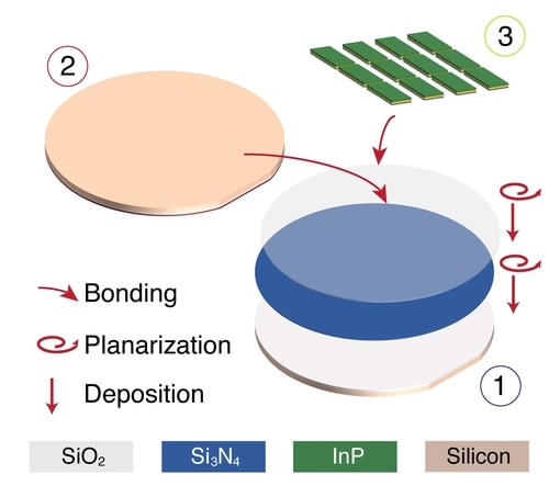
The method is mainly based on multiple wafer bonding of silicon and indium phosphide onto the Si3N4 substrate. Distributed feedback (DFB) lasers are fabricated on the silicon and indium phosphide layers. The single-frequency output from one DFB laser is delivered to a Si3N4 microresonator underneath, where the DFB laser seeds soliton microcomb formation and creates tens of new frequency lines.

This wafer-scale heterogeneous process can produce more than a thousand chip-scale soliton microcomb devices from a single 100-mm-diameter wafer, lending itself to commercial-level manufacturing. Each device is entirely electrically controlled. Importantly, the production level can be further scaled up to the industry standard 200- or 300-mm-diameter substrates.

“Our heterogenous fabrication technology combines the three mainstream integrated photonics platforms, namely silicon, indium phosphate, and Si3N4, and can pave the way for large-volume, low-cost manufacturing of chip-based frequency combs for next-generation high-capacity transceivers, data centers, sensing and metrology,” says Dr. Junqiu Liu who leads the Si3N4 fabrication at EPFL’s Center of MicroNanoTechnology (CMi).

UCF CFD model shows masks, ventilation stop COVID spread better than social distancing

Tyler O'Neal, Staff Editor MANUFACTURING April 5, 2021, 9:00 am

The results indicate masks and proper ventilation may be key to allowing more capacity in schools, businesses, and other indoor areas

A new study from the University of Central Florida suggests that masks and a good ventilation system are more important than social distancing for reducing the airborne spread of COVID-19 in classrooms.

The research, published recently in the journal Physics of Fluids, comes at a critical time when schools and universities are considering returning to more in-person classes in the fall.

"The research is important as it provides guidance on how we are understanding safety in indoor environments," says Michael Kinzel, an assistant professor in UCF's Department of Mechanical and Aerospace Engineering and study co-author.

"The study finds that aerosol transmission routes do not display a need for six feet social distancing when masks are mandated," he says. "These results highlight that with masks, transmission probability does not decrease with increased physical distancing, which emphasizes how mask mandates may be key to increasing capacity in schools and other places."

In the study, the researchers created a supercomputer model of a classroom with students and a teacher, then modeled airflow and disease transmission, and calculated airborne-driven transmission risk. For the study, the researchers created a supercomputer model of a classroom with students and a teacher, then modeled airflow and disease transmission, and calculated airborne-driven transmission risk.  CREDIT Michael Kinzel, UCF

The classroom model was 709 square feet with 9-foot-tall ceilings, similar to a smaller-size, university classroom, Kinzel says. The model had masked students -- any one of whom could be infected-- and a masked teacher at the front of the classroom.

The researchers examined the classroom using two scenarios -- a ventilated classroom and an unventilated one -- and using two models, Wells-Riley and Computational Fluid Dynamics. Wells-Riley is commonly used to assess indoor transmission probability and Computational Fluid Dynamics is often used to understand the aerodynamics of cars, aircraft, and the underwater movement of submarines.

Masks were shown to be beneficial by preventing direct exposure of aerosols, as the masks provide a weak puff of warm air that causes aerosols to move vertically, thus preventing them from reaching adjacent students, Kinzel says.

Additionally, a ventilation system in combination with a good air filter reduced the infection risk by 40 to 50% compared to a classroom with no ventilation. This is because the ventilation system creates a steady current of airflow that circulates many of the aerosols into a filter that removes a portion of the aerosols compared to the no-ventilation scenario where the aerosols congregate above the people in the room.

These results corroborate recent guidelines from the U.S. Centers for Disease Control and Prevention that recommend reducing social distancing in elementary schools from six to three feet when mask use is universal, Kinzel says.

"If we compare infection probabilities when wearing masks, three feet of social distancing did not indicate an increase in infection probability with respect to six feet, which may provide evidence for schools and other businesses to safely operate through the rest of the pandemic," Kinzel says.

"The results suggest exactly what the CDC is doing, that ventilation systems and mask usage are most important for preventing transmission and that social distancing would be the first thing to relax," the researcher says.

When comparing the two models, the researchers found that Wells-Riley and Computational Fluid Dynamics generated similar results, especially in the non-ventilated scenario, but that Wells-Riley underpredicted infection probability by about 29 percent in the ventilated scenario.

As a result, they recommend some of the additional complex effects captured in Computational Fluid Dynamics be applied to Wells-Riley to develop a more complete understanding of the risk of infection in space, says Aaron Foster, a doctoral student in UCF's Department of Mechanical and Aerospace Engineering and the study's lead author.

"While the detailed Computational Fluid Dynamics results provided new insights into the risk variation and distance relationships, they also validated the more commonly used Wells-Riley models as capturing the majority of the benefit of ventilation with reasonable accuracy," Foster says. "This is important since these are publicly available tools that anyone can use to reduce risk."

  1. New handle for controlling electromagnetic properties could enable spintronic supercomputing
  2. GW researchers develop fast, micrometer-size electro-optical modulator

Page 18 of 22

  • 13
  • 14
  • 15
  • 16
  • 17
  • 18
  • 19
  • 20
  • 21
  • 22
POPULAR RIGHT NOW
  • Alibaba’s superintelligence ambition puts supercomputing at the center of the AI race
    Alibaba’s superintelligence ambition puts supercomputing at the center of the AI race
  • AI’s trillion dollar compute race hits a hard limit: There isn’t enough power
    AI’s trillion dollar compute race hits a hard limit: There isn’t enough power
  • AI agents search 1.9 billion protein clusters, discover a new biological system
    AI agents search 1.9 billion protein clusters, discover a new biological system
  • Japan's AI supercomputer strategy starts with 400 MW of power
    Japan's AI supercomputer strategy starts with 400 MW of power
  • Supercomputing turns dark-matter waves into a testable prediction
    Artist's impression illustrating how wave-like density patterns produced by ultralight dark matter could warp space and alter the path of light from a distant source. As the light travels past the lensing object on its way to Earth, it follows a distorted path shaped by the surrounding mass distribution. The reflective sphere symbolizes the still-unknown nature of dark matter. The image was created using 3D computer graphics software. Credit: Amruth Alfred
    Artist's impression illustrating how wave-like density patterns produced by ultralight dark matter could warp space and alter the path of light from a distant source. As the light travels past the lensing object on its way to Earth, it follows a distorted path shaped by the surrounding mass distribution. The reflective sphere symbolizes the still-unknown nature of dark matter. The image was created using 3D computer graphics software. Credit: Amruth Alfred
  • Supercomputing the first stars: How MEGATRON reconstructed the chemical fingerprints of the early universe
    Supercomputing the first stars: How MEGATRON reconstructed the chemical fingerprints of the early universe
  • 15.6 Microseconds, 156 simulations: Supercomputing maps the moving machinery of an enzyme
    15.6 Microseconds, 156 simulations: Supercomputing maps the moving machinery of an enzyme
  • Who owns the AI supercomputer? Amazon may sell $8 billion of Nvidia Grace Blackwell chips, lease them back
    Who owns the AI supercomputer? Amazon may sell $8 billion of Nvidia Grace Blackwell chips, lease them back
  • The AI supercomputer has a new bottleneck: The community it needs to run in
    The AI supercomputer has a new bottleneck: The community it needs to run in
  • The AI supercomputer’s power problem is moving inside the rack: Delta pushes 800 VDC toward NVIDIA’s next generation
    The AI supercomputer’s power problem is moving inside the rack: Delta pushes 800 VDC toward NVIDIA’s next generation
THIS YEAR'S MOST READ
  • Wall Street wants to trade supercomputing power like oil
    Wall Street wants to trade supercomputing power like oil
  • Beamforming the future: BeammWave's 6G push signals the rise of orbital-terrestrial wireless networks
    Joakim Axmon
    Joakim Axmon
  • Silicon spintronics brings the P-computer closer to reality
    Microscope image of a semiconductor-integrated spintronic test chip developed by researchers at Tohoku University and NIST. The device demonstrates the first silicon-integrated probabilistic bit (p-bit), a key building block for future large-scale probabilistic computers designed for AI and optimization workloads.
    Microscope image of a semiconductor-integrated spintronic test chip developed by researchers at Tohoku University and NIST. The device demonstrates the first silicon-integrated probabilistic bit (p-bit), a key building block for future large-scale probabilistic computers designed for AI and optimization workloads.
  • AI breaks conservation barriers: Australia’s Wildlife Observatory leverages supercomputing to protect biodiversity
    AI breaks conservation barriers: Australia’s Wildlife Observatory leverages supercomputing to protect biodiversity
  • Hidden order, revealed at scale: Supercomputing, electron ptychography uncover the inner workings of relaxor ferroelectrics
    Hidden order, revealed at scale: Supercomputing, electron ptychography uncover the inner workings of relaxor ferroelectrics
  • Physics-trained ‘Digital Super Brain’ learns from supercomputers to accelerate discovery
    Physics-trained ‘Digital Super Brain’ learns from supercomputers to accelerate discovery
  • Cosmic ambition at scale: UK’s supercomputer unlocks a 2.5 petabytes universe
    Cosmic ambition at scale: UK’s supercomputer unlocks a 2.5 petabytes universe
  • Memory has become the new compute: Why Micron, SK Hynix crossing $1 trillion matters to supercomputing
    Memory has become the new compute: Why Micron, SK Hynix crossing $1 trillion matters to supercomputing
  • Huawei’s Tau Scaling ambition tests the limits of post-Moore semiconductor reality
    He Tingbo from HUAWEI delivered a keynote speech titled "New Semiconductor Path in Practice"
    He Tingbo from HUAWEI delivered a keynote speech titled "New Semiconductor Path in Practice"
  • Intel's Q1 results signal supercomputing surge driving Xeon momentum
    Intel's Q1 results signal supercomputing surge driving Xeon momentum
  • FRONTPAGE
  • LATEST
  • POPULAR
  • REGISTER
  • SOCIAL
  • VIDEO
  • SUBSCRIPTION
  • RSS
  • GUIDELINES
  • PRIVACY
  • TOS
  • ABOUT
  • +1 (816) 799-4488
  • editorial@supercomputingonline.com
© 2001 - 2026 SuperComputingOnline.com, LLC. All rights reserved. This material may not be published, broadcast, rewritten or redistributed without permission.
Sign In
  • FRONT PAGE
  • LATEST
    • MEDIA KIT
    • MOST READ
    • RSS FEED
    • ACADEMIA
    • AEROSPACE
    • APPLICATIONS
    • ASTRONOMY
    • AUTOMOTIVE
    • BIG DATA
    • BIOLOGY
    • CHEMISTRY
    • CLIENTS
    • CLOUD
    • DEFENSE
    • DEVELOPER TOOLS
    • EARTH SCIENCES
    • ECONOMICS
    • ENGINEERING
    • ENTERTAINMENT
    • HEALTH
    • INDUSTRY
    • INTERCONNECTS
    • GAMING
    • GOVERNMENT
    • MANUFACTURING
    • MIDDLEWARE
    • MOVIES
    • NETWORKS
    • OIL & GAS
    • PHYSICS
    • PROCESSORS
    • RETAIL
    • SCIENCE
    • STORAGE
    • SYSTEMS
    • VISUALIZATION
  • VIDEOS
    • ADD YOUR VIDEOS
    • MANAGE VIDEOS
  • COMMUNITY
    • TRADE SHOWS
    • SOCIAL NETWORK VIDEOS
    • SURVEYS
    • APPLICATIONS BROWSER
    • CONVERSATION INBOX
    • SOCIAL ADVERTISER
    • GROUPS
    • MARKETPLACE LISTINGS
    • PAGES
    • LEADERBOARD
    • POINTS LISTING
      • BADGES
    • PRIVACY CONFIRM REQUEST
    • PRIVACY CREATE REQUEST

Hey there! We noticed you’re using an ad blocker.