Memory has become the new compute: Why Micron, SK Hynix crossing $1 trillion matters to supercomputing

For decades, the supercomputing industry treated memory as a supporting technology, important, expensive, but ultimately secondary to processors. That hierarchy is now collapsing.
 
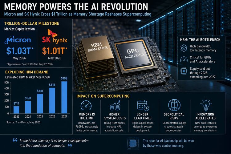
In a remarkable shift driven by the global artificial intelligence infrastructure race, memory manufacturers Micron Technology and SK Hynix have both surpassed $1 trillion in market capitalization, joining an elite tier once dominated almost exclusively by software giants, hyperscalers, and CPU designers.
 
The catalyst is not traditional DRAM demand from PCs or smartphones. It is the emergence of high-bandwidth memory (HBM) as the critical bottleneck in AI supercomputing systems.
 
In effect, the industry has discovered that compute acceleration without memory bandwidth is useless.

The memory crisis behind the AI boom

Modern AI supercomputers depend on massive parallel data movement. GPUs can perform extraordinary numbers of floating-point operations, but only if memory subsystems can continuously feed them data at sufficient speed.
 
That requirement has transformed HBM from a niche premium technology into the most strategically important component in the AI supply chain.
 
HBM stacks DRAM vertically and places it in close proximity to accelerators such as GPUs and AI ASICs, dramatically increasing memory bandwidth while reducing latency and power consumption. NVIDIA’s latest AI systems, for example, rely heavily on HBM capacity supplied primarily by Micron, SK Hynix, and Samsung Electronics.
 
The result is a structural supply shortage unlike previous semiconductor cycles.
 
Industry reports indicate that HBM production capacity is effectively sold out through 2026, with some supply commitments extending into 2027.
 
This shortage is now reshaping the economics of the entire HPC ecosystem.

Why is this different from previous memory cycles

Historically, memory markets were notoriously cyclical. Oversupply repeatedly crushed DRAM pricing, destroying margins and valuations.
 
Investors treated memory vendors as commodity manufacturers.
 
AI infrastructure is changing that assumption.
 
HBM manufacturing is vastly more complex than commodity DRAM. Advanced packaging, thermal constraints, TSV stacking, and proximity integration with accelerators create production limitations that cannot be expanded quickly. Each HBM stack also consumes substantially more wafer capacity than standard DRAM products.
 
This means supply elasticity has weakened precisely as demand has exploded.
 
The market is increasingly pricing memory manufacturers not as cyclical commodity vendors, but as strategic infrastructure gatekeepers. Reddit investor discussions, often an early indicator of broader retail sentiment, increasingly describe HBM suppliers as occupying “the AI toll booth.”
 
That language would have been unthinkable in semiconductor markets only three years ago.

The implications for supercomputing

For the supercomputing industry, the implications are profound.

1. Memory bandwidth is becoming the primary scaling constraint

Traditional HPC procurement focused primarily on FLOPS and interconnect performance. Increasingly, however, system architects are discovering that AI and exascale workloads are memory-bound rather than compute-bound.
 
Large language models, graph analytics, molecular simulation, weather forecasting, and multimodal AI systems all require enormous memory throughput.
 
This changes procurement priorities.
 
Future leadership-class supercomputers may be differentiated less by raw compute density and more by memory subsystem architecture and access efficiency.
 
The industry’s center of gravity is moving from processor-centric design toward memory-centric system engineering.

2. Supercomputer costs will rise

Persistent HBM shortages are already driving dramatic price increases in memory components.
 
Reuters reported memory pricing doubled in the first quarter of 2026, with further increases expected.
 
For HPC operators, this translates directly into higher system acquisition costs.
 
National laboratories, cloud providers, and enterprise AI operators may increasingly compete for the same limited pool of memory resources. That competition risks extending procurement lead times and delaying deployment schedules for new supercomputing systems.
 
In practical terms, memory may become the pacing factor for global AI infrastructure deployment.

3. The industry’s power structure is changing

For years, the semiconductor hierarchy revolved around CPU vendors and, later, GPU manufacturers.
 
Now, memory vendors are becoming strategic equals.
 
This is particularly important because the HBM market is highly concentrated. Micron, SK Hynix, and Samsung collectively dominate advanced memory production.
 
Such concentration introduces geopolitical and supply chain risk into the supercomputing ecosystem.
 
The United States increasingly views Micron as a strategic domestic supplier, while South Korea’s memory industry has become central to global AI infrastructure economics.
 
Future export controls, trade disputes, or manufacturing disruptions could therefore impact AI supercomputing capacity worldwide.

4. HPC architecture innovation will accelerate

The memory shortage is also likely to accelerate architectural innovation.
 
Researchers and vendors are already exploring:
  • Near-memory computing
  • Processing-in-memory architectures
  • CXL-based memory pooling
  • Optical interconnects
  • Advanced caching hierarchies
  • HBM alternatives and hybrid memory systems
The economics of memory scarcity will force the industry to become more efficient in data movement and memory utilization.
 
That could ultimately reshape software design as much as hardware engineering.

A warning sign for the AI infrastructure economy

There is, however, another way to interpret these trillion-dollar valuations.
 
They reflect not just technological progress, but also expose a new vulnerability in the AI ecosystem.
 
The AI industry now relies heavily on a handful of companies that can produce the advanced memory needed for cutting-edge accelerators. If memory supplies remain tight through 2027, as some industry leaders predict, the growth of AI infrastructure could stall regardless of GPU availability.
 
In this context, the soaring valuations of Micron and SK Hynix signal not just success, but the emergence of a new bottleneck for AI supercomputing.
 
While computing scarcity once dominated industry concerns, it is now clear that memory shortages could prove even more critical.
He Tingbo from HUAWEI delivered a keynote speech titled "New Semiconductor Path in Practice"

Huawei’s Tau Scaling ambition tests the limits of post-Moore semiconductor reality

For more than half a century, the semiconductor industry advanced according to a relatively simple premise: shrink transistors, increase density, improve performance. That principle, popularized as Moore’s Law, became the organizing framework behind modern computing, from smartphones to supercomputers.
 
Now, Huawei is proposing an alternative future.
 
At the 2026 IEEE International Symposium on Circuits and Systems (ISCAS) in Shanghai, Huawei unveiled what it calls the Tau (τ) Scaling Law, a new semiconductor scaling methodology the company claims could eventually deliver transistor density equivalent to 1.4-nanometer-class chips by 2031, even without access to extreme ultraviolet (EUV) lithography systems.
 
The announcement immediately attracted global attention because it directly challenges one of the central assumptions of the U.S.-China semiconductor conflict: that denying China access to advanced lithography tools would permanently constrain its ability to compete at the leading edge.
 
Huawei’s proposal suggests a different strategy altogether, one focused less on shrinking transistors geometrically and more on reducing signal propagation delay across increasingly complex computing systems.
 
Whether that strategy represents a genuine architectural breakthrough or an ambitious marketing reframing of already emerging packaging trends remains an open question.

The end of traditional scaling

Huawei’s argument begins from a premise many semiconductor engineers already accept: conventional transistor scaling is becoming economically and physically unsustainable.
 
Modern transistors are approaching atomic dimensions. Advanced nodes now face:
  • escalating fabrication costs
  • worsening thermal density
  • increasing interconnect bottlenecks
  • diminishing performance-per-node gains
Even leading-edge manufacturers such as Taiwan Semiconductor Manufacturing Company (TSMC) increasingly rely on advanced packaging, chiplets, backside power delivery, and 3D stacking to continue performance scaling.
 
Huawei’s Tau Scaling proposal attempts to formalize that transition into an entirely new scaling framework.
 
Instead of focusing primarily on transistor geometry, Tau Scaling emphasizes reducing the time it takes for signals and data to propagate through devices, circuits, chips, and systems.
 
The company describes this as “time (τ) scaling,” replacing geometric scaling as the core driver of semiconductor evolution.
 
Conceptually, the idea is not unreasonable.
 
Interconnect latency and data movement have increasingly become dominant constraints in modern computing systems, particularly in AI infrastructure and high-performance computing (HPC) environments.
 
The question is whether Huawei’s implementation can truly compensate for the absence of cutting-edge fabrication capability.

LogicFolding and the search for density without EUV

The practical embodiment of Huawei’s strategy is a chip architecture called LogicFolding.
 
According to Huawei, LogicFolding reduces resistive and capacitive signal loads by shortening internal wiring distances and restructuring logic layouts.
 
The company claims this approach could eventually enable transistor density “equivalent” to 14-angstrom (1.4 nm) process technologies by 2031.
 
Importantly, Huawei is not claiming it can manufacture physical 1.4 nm transistors using domestic lithography.
 
That distinction matters enormously.
 
The company is instead arguing that architectural efficiency, stacking methods, and interconnect optimization can produce system-level density and performance comparable to future leading-edge nodes without requiring equivalent fabrication precision.
 
This is where skepticism becomes unavoidable.

Equivalent to 1.4 nm is not 1.4 nm

The semiconductor industry has already begun moving beyond simple node naming conventions. Modern “3 nm” or “2 nm” branding often reflects marketing terminology rather than literal transistor gate dimensions.
 
Still, there remains a substantial difference between:
  • true leading-edge fabrication capability
  • and architectural techniques designed to compensate for older manufacturing processes
Huawei’s claims rely heavily on the latter.
 
Independent analysts note that the company has not yet provided:
  • fabrication yield data
  • thermal performance benchmarks
  • manufacturing cost curves
  • detailed lithography pathways
  • large-scale production validation
That absence is significant because advanced packaging and 3D stacking introduce their own engineering penalties, including:
  • thermal dissipation challenges
  • reduced manufacturing yields
  • power delivery complexity
  • signal integrity issues
  • increased packaging cost
In effect, Huawei may be reframing a broader industry transition toward heterogeneous integration as a proprietary scaling “law.”

The geopolitical semiconductor reality

Still, dismissing Huawei outright would be shortsighted.
 
The company has repeatedly demonstrated an ability to survive technological restrictions many analysts initially considered existential. Since being placed on the U.S. Entity List in 2019, Huawei has:
  • rebuilt smartphone SoC capabilities
  • developed domestic AI accelerators
  • expanded its Ascend AI platform
  • helped drive China’s semiconductor self-sufficiency efforts
Huawei says it has already designed and mass-produced 381 chips based on Tau Scaling concepts over the past six years.
 
Its upcoming Kirin processors scheduled for late 2026 will reportedly become the first commercial chips to adopt LogicFolding architecture.
 
That means the industry will soon gain its first real-world test of whether Huawei’s claims translate into meaningful gains in:
  • power efficiency
  • thermal stability
  • sustained AI performance
  • memory bandwidth
  • real application throughput
Until shipping silicon exists at scale, Tau Scaling remains more roadmap than proof.

HPC, AI, and the real semiconductor bottleneck

Ironically, Huawei’s emphasis on interconnect latency may align with broader industry realities more closely than some critics admit.
 
Modern AI supercomputers increasingly struggle less with raw transistor density than with:
  • memory movement
  • inter-GPU communication
  • network latency
  • power delivery
  • cooling efficiency
In hyperscale AI clusters, data movement often consumes more energy than arithmetic itself.
 
Huawei’s Tau Scaling framework explicitly targets these system-level bottlenecks.
 
The company says the architecture will eventually expand beyond smartphones into:
  • Ascend AI accelerators
  • SuperPod AI clusters
  • unified memory systems
  • large-scale datacenter infrastructure
That direction mirrors broader industry trends already visible across:
  • NVIDIA’s NVLink ecosystems
  • AMD chiplet architectures
  • advanced CoWoS packaging systems
  • wafer-scale AI accelerators
In other words, Huawei may not be inventing an entirely new semiconductor paradigm so much as accelerating an inevitable post-Moore architectural transition under geopolitical pressure.

A new law, or a new narrative?

The semiconductor industry has seen many proposed successors to Moore’s Law over the decades.
 
Few survived commercial reality.
 
Huawei’s Tau Scaling Law may ultimately prove to be:
  • a meaningful systems-engineering framework
  • a strategic branding exercise
  • or a partial workaround for lithography limitations
Possibly all three simultaneously.
 
While skepticism towards Huawei's announcement is warranted due to the lack of independent validation and its largely aspirational claims, the broader industry context makes it hard to dismiss.
 
The era of semiconductor advancement solely relying on transistor miniaturization is clearly over. Future improvements will increasingly depend on architecture, interconnect design, advanced packaging, software optimization, and system-level orchestration.
 
Huawei's announcement might not invalidate Moore's Law, but it does reveal an important shift in the global semiconductor industry: the future of computing performance will likely hinge less on creating the smallest transistors and more on designing the most efficient systems around them.
Joakim Axmon
Joakim Axmon

Beamforming the future: BeammWave's 6G push signals the rise of orbital-terrestrial wireless networks

Wireless networking is moving beyond just terrestrial cellular towers or satellite constellations. The next generation of communications infrastructure is aiming for something much more advanced: a fully integrated system that combines both ground-based and orbital networks. This new ecosystem will be driven by intelligent beamforming, AI-powered spectrum management, and software-defined radio technologies.
 
This transition took a major step forward when BeammWave announced that digital beamforming is now officially being considered in the 3GPP standardization process, following the RAN4#119 meeting in Dalian, China.
 
While the announcement may appear narrowly technical, its implications extend far beyond conventional telecom engineering. The move represents a deeper transformation underway across the global communications landscape, one in which terrestrial 6G systems and low Earth orbit (LEO) satellite constellations increasingly converge into a unified computational network fabric.
 
"Bringing Digital Beamforming to the standardization table is a critical step forward in addressing the reliability and performance of high-frequency FR2 networks," says Joakim Axmon, Senior Expert Systems and Standards at BeammWave. "We look forward to continuing this work alongside the ecosystem to drive the digital evolution of 6G, ensuring future networks are both technically robust and commercially viable."

The digital beamforming inflection point

For decades, high-frequency wireless systems have struggled against the harsh realities of physics.
 
Millimeter-wave (mmWave) frequencies above 24 GHz offer enormous bandwidth potential, but they suffer from:
  • Severe signal attenuation
  • Limited propagation range
  • Sensitivity to environmental obstruction
  • Complex mobility management challenges
Early 5G deployments addressed these issues using analog beamforming, steering radio signals directionally toward users. But analog approaches remain constrained in flexibility and scalability.
 
BeammWave’s proposal pushes the industry toward fully digital beamforming, in which beam steering is dynamically controlled by software rather than hardware-limited.
 
The company’s architecture combines:
  • Integrated radio chips
  • Embedded antennas
  • Proprietary signal-processing algorithms
  • Software-driven beam control
designed specifically for future 5G evolution and 6G deployments operating in Frequency Range 2 (FR2).
 
According to the press release, 3GPP will now formally evaluate whether digital beamforming should become part of the standardized UE RF architecture for future 6G systems.
 
That evaluation may ultimately shape the technological foundation of global wireless infrastructure for the next decade.

Why beamforming matters more than ever

At first glance, beamforming appears to be a radio engineering problem.
 
In reality, it is becoming a computational problem.
 
Modern digital beamforming systems require:
  • Massive real-time signal processing
  • Adaptive multi-user optimization
  • AI-assisted interference mitigation
  • Dynamic spectrum allocation
  • Continuous spatial recalibration
Future 6G networks may involve thousands of simultaneous directional beams operating cooperatively across dense urban environments.
 
This transforms wireless networking into a distributed supercomputing challenge.
 
As a result, future telecommunications infrastructure will increasingly depend on:
  • AI accelerators
  • Edge computing systems
  • Advanced RF semiconductors
  • Real-time optimization algorithms
  • High-performance networking architectures
In many respects, next-generation wireless systems are evolving into planetary-scale distributed computing platforms.

The satellite convergence era

At the same time terrestrial wireless evolves, satellite internet constellations are rapidly reshaping global connectivity.
 
Systems such as:
  • Starlink from SpaceX
  • Amazon’s low Earth orbit (LEO) satellite network
have demonstrated that low Earth orbit satellite networks can deliver broadband-class connectivity with latency low enough for real-time applications.
 
However, despite growing speculation, LEO constellations are unlikely to replace terrestrial 5G or 6G infrastructure outright.
 
Instead, the industry is moving toward convergence.
 
Terrestrial networks remain vastly superior for:
  • Dense urban capacity
  • Indoor connectivity
  • Ultra-low-latency applications
  • High spectral reuse
  • Edge AI integration
LEO systems excel at:
  • Global coverage
  • Rural connectivity
  • Maritime and aviation communications
  • Disaster resilience
  • Universal fallback networking
The future architecture increasingly appears hybrid rather than competitive.

Non-terrestrial networks become core infrastructure

3GPP’s long-term vision for 6G already incorporates the concept of Non-Terrestrial Networks (NTN), an integrated framework in which satellites, terrestrial cells, airborne systems, and edge computing resources operate seamlessly together.
 
Within that vision:
  • Smartphones dynamically switch between terrestrial and orbital links.
  • AI systems optimize routing in real time.
  • Beamforming systems coordinate across ground and space networks.
  • Spectrum becomes software-defined and adaptive.
Digital beamforming becomes central to making this architecture practical.
 
The same adaptive directional communication technologies being explored for terrestrial 6G mmWave deployments are equally essential for:
  • Satellite phased arrays
  • Inter-satellite laser communications
  • Direct-to-device satellite networking
  • Dynamic orbital spectrum reuse
The distinction between “cell tower” and “satellite node” may eventually become largely architectural rather than functional.

Solving the economics of 6G

One of the most important aspects of the BeammWave initiative is its focus on cost and power efficiency.
 
Historically, digital beamforming was considered impractical for mobile systems due to:
  • High power consumption
  • RF front-end complexity
  • Thermal limitations
  • Semiconductor integration challenges
But advances in silicon integration, signal processing efficiency, and AI-driven radio management are beginning to change that equation.
 
The 3GPP evaluation will specifically study:
  • Commercial power envelopes
  • Device implementation costs
  • Base station architecture impacts
  • Radio Resource Management requirements
  • Overall system integration procedures
These studies are crucial because future 6G networks will require unprecedented deployment density and computational coordination.
 
Without breakthroughs in efficiency, the economics of large-scale 6G infrastructure would become difficult to sustain.

Communications as a computational ecosystem

The deeper significance of this moment is philosophical as much as technical.
 
Wireless networking is no longer simply about transmitting signals between devices.
 
It is becoming a unified computational ecosystem spanning:
  • Terrestrial infrastructure
  • Orbital networks
  • AI-driven edge systems
  • Distributed compute resources
  • Software-defined spectrum management
In this emerging architecture, connectivity itself becomes intelligent.
 
Beamforming systems will continuously adapt to user movement, atmospheric conditions, orbital positioning, and network congestion in real time.
 
The network will increasingly think.

The inspirational horizon of 6G

The inclusion of digital beamforming in formal 3GPP discussions signals more than a standards milestone.
 
It reflects an industry beginning to reimagine the very nature of global communications.
 
Future wireless systems may no longer be bound by geography, infrastructure ownership, or even the distinction between Earth and orbit. Instead, they may function as a continuous intelligent fabric connecting satellites, cities, autonomous systems, industrial infrastructure, and billions of devices simultaneously.
 
What BeammWave and the broader 6G ecosystem are helping build is not simply a faster wireless network.
 
It is the foundation for a globally distributed, computationally intelligent communications layer capable of spanning the planet, and eventually, perhaps far beyond it.