CLOUD
Fujitsu Laboratories Develops Record-Breaking 56 Gbps Receiver Circuit for Communications between CPUs

Doubles data-communications speeds, contributing to the next generation of high-performance servers and supercomputers
Fujitsu Laboratories has announced the development of a receiver circuit capable of receiving communications at 56 Gbps. This marks the world's fastest data communications between CPUs equipped in next-generation servers.
In recent years, raising data-processing speeds in servers has meant increasing CPU performance, together with boosting the speed of data communications between chips, such as CPUs. However, one obstacle to this has been improving the performance of the circuits that correct degraded waveforms in incoming signals.
Fujitsu Laboratories has used a new "look-ahead" architecture in the circuit that compensates for quality degradation in incoming signals, parallelizing the processing and increasing the operating frequency for the circuit in order to double its speed.
This technology holds the promise of increasing the performance of next-generation servers and supercomputers.
Details of this technology are being presented at the 2014 Symposia on VLSI Technology and Circuits, opening June 9 in Hawaii (VLSI Circuits Presentation 11-2).
Background
In order to enhance the performance of datacenters underpinning the spread of cloud computing in recent years, a need has arisen for servers that process data faster. While this can be achieved partly through faster CPUs, large-scale systems connecting many CPUs are also being built, and the amount of data transmitted, either within the same CPU-equipped chassis or across separate chassis, is growing dramatically. To cope with these volumes, data communication speeds in the current generation of servers is increasing from a few gigabits per second today to ten or more gigabits per second. Because it is anticipated that data processing volumes will continue to experience explosive growth, however, for the next generation of high-performance servers, the goal is to double current levels to 56 Gbps. Furthermore, the Optical Internetworking Forum (OIF) is moving forward on the standardization of 56 Gbps for the optical modules used for optical transmission between chassis.
Issues
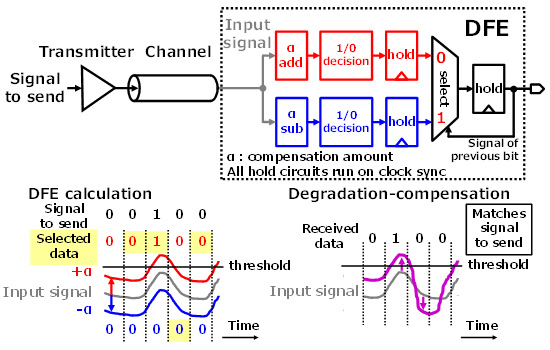
An effective way to speed up the receiver circuit is to improve the processing performance of the decision feedback equalizer (DFE) circuit that compensates for the degraded input-signal waveform (Figure 2).The principle behind DFE is to correct the input signal based on the bit-value of the previous bit and to emphasize changes in the input signal, but the actual circuit design works by choosing between two predefined corrected candidates. If the previous bit value was a 0, the correction process would apply a positive correction to the input signal (additive) to emphasize the change from 0 to 1. If the previous bit value was 1, it would apply a negative correction to the input signal (subtractive) to emphasize the change from 1 to 0. If another 0 was received, the positive compensation would increase the signal level, but not to such a level as would create a problem for the 1/0 decision circuit.
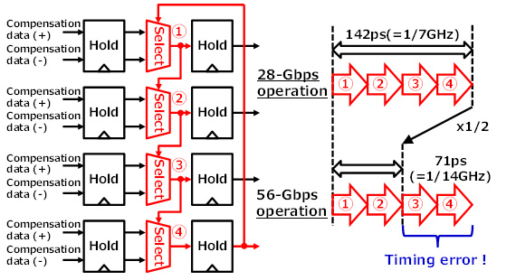
In ordinary circuit designs that run at 56 Gbps, there are 16 DFE circuits coupled together. Using 4 DFE circuits as an example, they run at 1/4th the actual frequency. So for 28-Gbps communications rates, 1/4th of that is 142 picoseconds, and four bits-worth of compensation can be applied during that interval. But at 56 Gbps, 1/4th of that speed amounts to 71 picoseconds, during which time only 2 bits-worth of compensation can be applied, resulting in timing errors (Figure 3).

Figure 2: The decision feedback equalizer, a key technology, and its role in accelerating communications

Figure 3: Real-world architecture of conventional DFE and problems it encounters at 56 Gbps
Technology
Fujitsu Laboratories took a new approach, a "look-ahead" method that can be implemented as a parallel process, pre-calculating two candidates based on the selection result for the previous bit, and simultaneously deciding the value of the previous bit and the current bit after deciding the value of the bit two bits previous. This shortens calculation times, resulting in a receiver circuit that can operate at 56 Gbps (Figure 4).
Features of the new technology are as follows:
1. Look-ahead compensation process
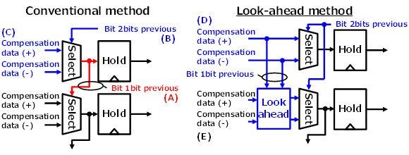
In the existing method, the result of the previous bit's selection circuit (A) is implemented by a circuit combining the result of the selection circuit for the bit two bits previous (B) and the input signal for the selection circuit one bit previous (+/- compensation data) (C). In the look-ahead method, the input signal for the selection circuit one bit previous (+/- compensation data) (D) and the input signal for the selection circuit of the current bit (+/- compensation data) (E) are combined using a look-ahead circuit, and candidates for the selection circuit are pre-computed. Doing this relies on only the result from the selection circuit for the bit two bits previous, without using the result from the selection circuit for the bit one bit previous, while functioning essentially the same as the existing method.

Figure 4: The principle of the look-ahead method
2. Parallelized look-ahead processing using a hold circuit
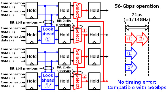
Multiple look-ahead circuits that apply DFE one bit at a time can operate independently (Figure 5). Fujitsu Laboratories inserted a hold circuit between the selection circuit and look-ahead circuit, with the input and output of each hold circuit being synchronized, making it possible to parallelize these processes.
Because the calculation time for the look-ahead circuit is roughly the same as the selection time for the selector, overall calculation time is dependent on the number of selectors deciding based on data from two bits previous, so in a four-bit structure, that would be two. Running at 1/4th of 56 Gbps allows computations to be safely completed within 71 picoseconds. This makes it possible to receive data at 56 Gbps, doubling existing communications speeds.

Figure 5: The new architecture for DFE and its results
Results
This technology makes it possible to increase bandwidth of communications between CPUs in future servers and supercomputers, even if CPU performance doubles, without increasing pin counts, and will contribute to increased performance in large-scale systems where numerous CPUs are interconnected. In addition, it complies with standards for optical-module communications, and compared to the 400-Gbps Ethernet in OIF-CEI-28G optical-module communications, the number of circuits running in parallel (number of lanes) can be halved, allowing for smaller optical modules running on less power, and higher system performance.
Future Plans
Fujitsu Laboratories plans to apply this technology to the interfaces of CPUs and optical modules, with the goal of a practical implementation in fiscal 2016. The company is also considering applications to next-generation servers, supercomputers, and other products.

